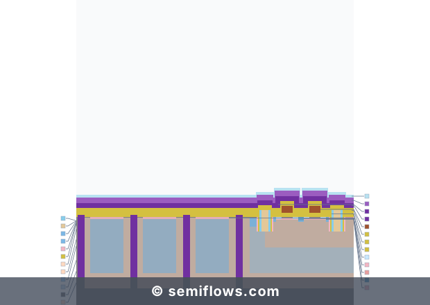
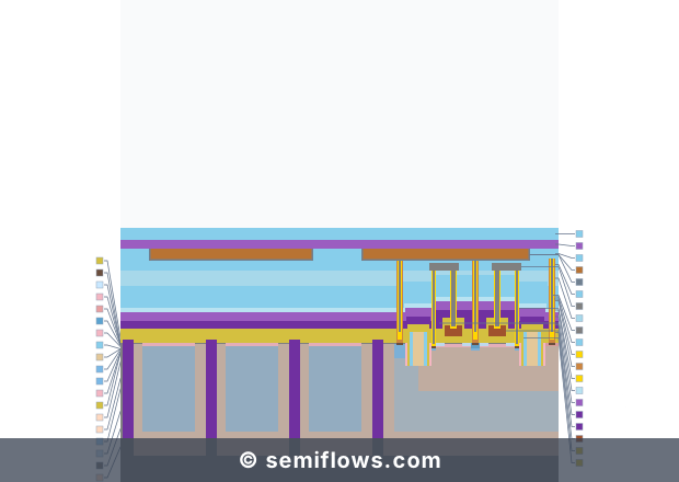
Introduction
In semiconductor manufacturing, deposition rate—defined as the thickness of thin film deposited on a substrate per unit of time—is a foundational process metric . It directly governs tool throughput, thermal budget, and overall manufacturing cost, while establishing critical constraints for film quality and uniformity (Engineering Practice). Controlling the deposition rate is essential across a wide spectrum of technologies, ranging from high-throughput physical vapor deposition (PVD) and chemical vapor deposition (CVD) to highly controlled atomic layer deposition (ALD) processes .
Achieving the optimal deposition rate requires balancing productivity with structural and electrical requirements . For instance, in deep-submicron features, an excessively high deposition rate can lead to keyholes, voids, or non-conformal step coverage, whereas an excessively slow rate reduces tool efficiency and exposes the substrate to prolonged thermal or plasma stress [P2, P4]. This article explores the physical and chemical principles that dictate deposition rates, analyzes how key process parameters affect film growth, and details how deposition kinetics have evolved to support advanced technology nodes .
Physics & Mechanism
Kinetics and Transport Regimes
Thin-film deposition from the gas phase is fundamentally governed by a series of sequential transport and reaction steps [P2, T1]:
- Mass transport of precursor molecules from the bulk gas flow through the boundary layer to the substrate surface .
- Adsorption of reactant species onto active surface sites (Engineering Practice).
- Chemical reactions or surface migration (diffusion) of the adsorbed species .
- Desorption of volatile reaction byproducts (Engineering Practice).
- Bulk transport of byproducts away from the boundary layer (Engineering Practice).
The overall deposition rate is determined by the slowest step in this chain, establishing two primary operating regimes: the surface-kinetics-limited regime and the mass-transport-limited regime .
In the surface-kinetics-limited regime, mass transfer through the boundary layer is rapid compared to the chemical reactions occurring at the surface . Under these conditions, the deposition rate ($R$) is determined by the surface reactant concentration ($C_s$) and the surface reaction rate constant ($k_s$), expressed as:
$$R = k_s C_s$$
Because the rate constant ($k_s$) follows an Arrhenius behavior, this regime is highly sensitive to temperature variations (Engineering Practice).
Conversely, in the mass-transport-limited (or diffusion-limited) regime, surface reactions occur faster than the rate at which reactants can diffuse through the boundary layer . Here, the deposition rate is governed by the diffusion coefficient ($D$) of the precursor and the boundary layer thickness ($\delta$):
$$R = \frac{D}{\delta}(C_g - C_s)$$
where $C_g$ represents the bulk gas-phase concentration of the reactant . In this regime, the deposition rate is highly dependent on gas flow dynamics and reactor geometry, but relatively insensitive to temperature changes .
Sputtering and Evaporation Physics
For physical deposition methods, the growth rate mechanisms depend on physical vaporization and transport [P3, T1]. In thermal or electron-beam evaporation, the emission of species from a source is modeled by the Knudsen cosine distribution law . The local deposition rate ($v$) on a substrate at a distance ($r$) from a planar source depends on the evaporation rate ($R_{\text{evap}}$), the emission angle ($\theta_k$), and the receiver angle ($\theta_i$):
$$v = \frac{R_{\text{evap}} \Omega}{\pi r^2} \cos \theta_k \cos \theta_i$$
In sputtering PVD, high-energy ions within a plasma bombard a target, transferring momentum to eject target atoms . The deposition rate is primarily determined by the sputter yield—defined as the number of target atoms ejected per incident ion—which depends on ion energy, ion mass, and target material bonding configurations [P3, A1].
Process Principles
Process parameters directionally influence deposition rates by altering gas-phase kinetics, plasma density, and surface energy [P1, P2].
Temperature and Pressure Interactions
In chemical deposition processes (e .g., atmospheric pressure CVD or low-pressure CVD), raising the substrate temperature exponentially increases the surface reaction rate constant, driving higher deposition rates in the surface-kinetics-limited regime . However, at elevated temperatures, gas-phase depletion of the reactants can occur along the reactor path as precursors are consumed upstream, leading to a down-stream decrease in deposition rate .
In physical processes like magnetron sputtering, increasing the substrate temperature often increases the surface migration of deposited atoms, which can densify the film but sometimes yields a lower apparent deposition rate due to localized desorption or restructuring [P1, P3]. Working pressure also plays a dual role: increasing the working pressure shortens the mean free path of sputtered or reactive species, increasing gas-phase collisions . At moderate pressures, this enhances ionization and secondary electron emission, raising the deposition rate; however, at excessively high pressures, severe collisional scattering reduces the kinetic energy of the species, causing fewer atoms to reach the substrate and lowering the net deposition rate .
Power and Precursor Flow
In plasma-enhanced chemical vapor deposition (PECVD) and sputtering, radio frequency (RF) or direct current (DC) power determines the plasma density and dissociation efficiency of precursors [P1, A2]. Increasing the power boosts the generation rate of reactive radicals and ions, directionally raising the deposition rate [P1, A2]. Concurrently, the flow rate of the precursor gases directly defines the concentration gradient within the boundary layer; under mass-transport-limited conditions, elevating precursor flow rates scales the deposition rate linearly until the process transitions into a surface-saturation or reaction-limited regime .
Challenges & Failure Modes
Aspect Ratio Dependent Deposition and Voids
As feature dimensions shrink, depositing conformal films in high aspect ratio (HAR) trenches becomes increasingly difficult . Precursors or sputtered atoms face transport resistance when entering narrow trenches, leading to higher deposition rates at the top corners than at the bottom of the structure . This geometric shadowing causes premature top sealing, trapping reactant gases or creating unfilled gaps known as voids [A1, A2].
To mitigate this, processes use modulated dual-power RF duty cycles to balance deposition and simultaneous in-situ etching, removing excess material from the trench opening to keep the pathway open . Additionally, utilizing high molecular weight (HMW) precursors can minimize the sputter-yield backscattering of incoming ions, keeping the net deposition rate closely aligned with the reactant dose rate .
Gas Depletion and Non-Uniformity
In batch-type furnace reactors, precursor depletion along the gas flow path poses a significant challenge . As reactant gases flow across heated wafers, they are continuously consumed, reducing the local reactant concentration downstream . If not compensated for, this depletion causes a systematic drop in the deposition rate from the inlet to the exhaust end of the process chamber . Engineers counteract this by introducing temperature ramps (slightly increasing the temperature zone-by-zone downstream) to accelerate reaction kinetics and compensate for the depleted gas concentration .
Loss of Selective Growth
In advanced metallization, such as selective chemical vapor deposition of ruthenium (Ru) for barrier-free contacts, deposition rates must be tightly controlled to favor metal surfaces over surrounding dielectrics . If the cleaning processes prior to deposition are insufficient, or if the process window drifts, the selectivity of the deposition rate between the metal and the dielectric breaks down, leading to undesired nucleation on dielectric surfaces and subsequent electrical leakage .
Technology Node Evolution
28nm Planar Era
At the 28nm Planar Flow node, traditional CVD and PVD methods operated at high deposition rates to maintain high fab throughput . Planar gate stacks transitioned to high-k metal gate (HKMG) structures, where ultra-thin dielectric layers required the atomic-level thickness precision of ALD . While ALD deposition rates are inherently low because they rely on self-limiting surface reactions, the planar geometries permitted relatively straightforward integration with batch-processing equipment .
14nm FinFET Node
The transition to the 14nm FinFET node introduced highly three-dimensional fin field effect transistor (FinFET) architectures, where traditional line-of-sight PVD processes suffered from severe shadowing and non-uniform deposition rates on fin sidewalls (Engineering Practice). To achieve conformal coverage, conformal PECVD and ALD processes became critical for spacer definition, gate oxides, and conformal doping layers (Engineering Practice).
7nm and Beyond
At the 7nm FinFET node and sub-5nm gate-all-around (GAA) architectures, lithography relied heavily on multi-patterning schemes and extreme ultraviolet (EUV) lithography (Engineering Practice). For these advanced structures, deposition rates are no longer evaluated solely as bulk thickness over time; they are instead optimized for spatial selectivity, atomic layer precision, and anisotropic directionality [A1, A3]. Highly selective deposition rates on specific metal or dielectric surfaces (area-selective deposition) prevent registration and alignment errors during self-aligned contact (SAC) fabrication .
| Process Node | Key Structural Challenge | Deposition Rate Strategy | Primary Deposition Technology |
|---|---|---|---|
| 28nm | Planar Gate Scale | High bulk deposition rates, initiation of ultra-thin HKMG control | CVD, PVD, thermal ALD (Engineering Practice) |
| 14nm | 3D Fin Conformality | Balanced step coverage over vertical sidewalls; avoidance of top-heavy pinching | Conformal PECVD, ALD (Engineering Practice) |
| 7nm and Beyond | Extremely tight pitches, SAC alignment, nanosheet gate wrap-around | Area-selective deposition, directional ion-beam deposition, low-temperature radical ALD | Selective CVD, Directional PVD, PE-ALD [A1, A3] (Engineering Practice) |
Related Processes
Deposition processes are highly integrated with adjacent manufacturing steps:
- Planarization: Deposition rates directly affect the incoming topography for chemical mechanical planarization (CMP) (Engineering Practice). Over-deposition increases CMP polish times and defect rates, whereas under-deposition leads to unpolished low spots (Engineering Practice).
- Patterning: In spacer-defined double patterning, the conformal deposition rate determines the spacer thickness, which directly translates to the critical dimension (CD) of the etched features .
- Etching: The selectivity of the dry etching process depends on the density and quality of the deposited hardmask films . Highly dense films deposited at lower, optimized rates offer superior etch resistance .
- Metallization: In back-end-of-line (BEOL) routing, such as copper dual damascene structures, the barrier/seed deposition rate controls the conformal coverage inside trenches, which is critical for subsequent electroplating .
Future Outlook
As the semiconductor industry advances toward 3D DRAM and high-aspect-ratio 3D NAND structures, controlling the deposition rate under extreme geometry constraints is paramount . The future lies in further refining area-selective deposition (ASD) and atomic layer epitaxy, where chemical inhibitors are used to tune local deposition rates down to zero on non-target materials, allowing bottom-up, defect-free growth . Additionally, integrating advanced in-situ diagnostics, such as real-time spectroscopic ellipsometry, allows for instantaneous monitoring of deposition rate transients, enabling closed-loop chamber control to meet the sub-angstrom tolerances of future technology nodes .