Process flow visualization
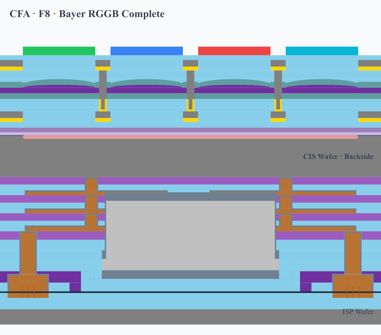
4 technology nodes · 40nm→7nm · 2.5D cross-sections
- Step-by-step flow navigation
- 2.5D cross-section for every step
- Rationale + citation tracing
A real 40nm starting point
Wafer In
40nm · Step 1 · Wafer Start
Complete 40nm→7nm flows, rendered step by step in 2.5D cross-sections, with an AI that follows the real sequence and shows paper, patent, and textbook sources when evidence covers the answer.
Process flow visualization
4 technology nodes · 40nm→7nm · 2.5D cross-sections
A real 40nm starting point
Wafer In
40nm · Step 1 · Wafer Start
Ångström Guide
40nm six-chapter structural guide
See the route first
trench isolation → pinned photodiode → completed frontside circuitry and wafer bond → backside thinning → CFA color selection → microlens focusing. Here, structure includes visible films and interfaces as well as doped regions such as P-pinning, whose geometry is subtle but whose surface-potential effect is decisive.
What this route helps you understand
How does 40nm BSI move from pixel isolation and the photosensitive junction through frontside circuitry, wafer bonding, and backside thinning to CFA color selection and microlens focusing?
Structural milestones
All 6 chapters
Process visualization, source tracing, and mechanism analysis work together at every step
Navigate 1,700+ steps across 40nm CIS, 28nm, 14nm, and 7nm flows, with live 2D process cross-sections showing how the material stack develops at every node
Q&A retrieves from curated papers, patents, and textbooks, with [T1][P2][A3] citations that expand to bibliographic details and available abstracts
Connects each step's process type, functional role, and surrounding flow context to explain physical, chemical, and integration mechanisms
Two parallel offerings — mix freely: process-flow nodes (one-time, lifetime) + AI deep Q&A (subscription, free tier included)
All nodes lifetime access + Pro AI for 1 year (45× Free AI usage each billing period)
One-time purchase, no automatic renewal. After one year, subscribe to Pro AI separately at the then-current annual price
Lifetime node content with one purchase; AI Pro is a separate subscription
Use the Fin Recess Etch example to follow changes to the fin and STI surfaces, then explore the step’s purpose and process risks.
See a real examplePreview selected examples. Purchase lifetime access to all 714 steps. Pro AI is available separately.
Compare isolation, gate, and contact integration across 28nm planar devices and 14nm/7nm FinFETs.
Unlocks 28nm + 14nm + 7nm with lifetime access to the complete flows.
Includes Owner AI usage. Pro AI subscription is separate.
Every technology node includes Owner: 3× Free AI usage each billing period · Rationale & risk analysis per step · Paper & patent citation tracing · 2.5D process cross-section for every step — physical structure evolution, step by step · One-time purchase, lifetime access
Available payment methods are shown at checkout
Loading prices for your billing region…
More AI usage; paid node content is purchased separately
Renews annually
Renews monthly for flexibility
Multiples compare standard billing-period usage allowances with Free (1×), excluding bonuses. Usage varies with the model, conversation length, and retrieval—not a fixed number of messages.
Pro upgrades AI Q&A; paid process-flow nodes remain separate purchases
Available payment methods are shown at checkout
Loading prices for your billing region…
14-day money-back guarantee · All payments are processed by Paddle.com as the Merchant of Record, handling payment processing, tax calculation, and invoicing. Paddle Buyer Terms
Common questions about the SemiFlows platform
SemiFlows is an AI-powered semiconductor process knowledge platform that provides complete, step-by-step process flows from 40nm to 7nm, covering both logic chips and CMOS image sensors. It integrates extensive research papers, patents, and authoritative textbooks to deliver in-depth rationale analysis with citation tracing for each process step. The 40nm BSI CIS flow is entirely free.
SemiFlows currently covers four process flows: 40nm BSI CMOS Image Sensor (417 steps, free), 28nm Planar (266 steps), 14nm FinFET (362 steps), and 7nm FinFET (714 steps). Together, these flows provide over 1,700 detailed process steps spanning both logic chip and image sensor fabrication.
SemiFlows is purpose-built for learning and researching semiconductor processes. It brings structured process flows, step-by-step cross-sections, physical and chemical mechanism explanations, and traceable paper and patent citations into one learning path, with Q&A grounded in the current step and surrounding flow context.
SemiFlows provides physics and chemistry principles behind each process step, mechanism explanations (why a process works), integration rationale (why steps are ordered a certain way), and risk analysis. All content focuses on fundamental principles — not specific manufacturing recipes, equipment parameters, or vendor details.
Yes. SemiFlows supports both English and Chinese (中文). Users can switch languages at any time using the language toggle. The AI chat assistant also responds in the user's selected language.