Introduction
In the relentless drive of Moore's law, scaling down the physical dimensions of integrated circuits has pushed optical lithography to its physical limits . As transistors transitioned from planar architectures to three-dimensional structures, such as the fin field effect transistor (FinFET), the spatial tolerances for critical features shrunk drastically . Among these features, the electrical contact that links the active source and drain regions of a transistor to the back-end-of-line (BEOL) metallization is one of the most challenging to pattern . This challenge is addressed through a technique known as self-aligned contact (SAC) .
Traditionally, contact vias were defined using direct lithographic patterning, which required a significant physical margin between the contact plug and the adjacent gate electrode to prevent accidental electrical short-circuits . However, as the gate pitch scaled down, the overlay error (the alignment accuracy of the scanner) began to exceed the available alignment budget . In response, the semiconductor industry introduced the SAC process at advanced technology nodes . By leveraging material selectivity instead of lithographic overlay precision, SAC allows contacts to be successfully landing on the source/drain regions even when the contact lithography mask is intentionally or unintentionally shifted over the gate . This process decoupling allows transistor gate width and contact size to be optimized independently for electrical performance, resolving one of the primary roadblocks in sub-22nm scaling .
Physics & Mechanism
At the heart of the self-aligned contact (SAC) process lies the physical and chemical principles of highly selective dry etching . In a typical SAC integration scheme, the gate electrode is capped with a protective dielectric layer, and the sidewalls are protected by a gate spacer, typically made of silicon nitride ($SiN_x$) . The interlayer dielectric (ILD) surrounding the gate stack is typically made of silicon dioxide ($SiO_2$) . The fundamental requirement of the SAC etch is to remove the $SiO_2$ layer to open the contact hole while leaving the protective $SiN_x$ cap and spacer intact .
This material selectivity is achieved through fluorocarbon-based plasma chemistry, operating on the principles of ion-assisted chemical etching and surface polymerization . During the plasma process, fluorocarbon precursors ($C_xF_y$) fragment into reactive radicals and ions . These species interact differently with $SiO_2$ and $SiN_x$ surfaces:
1 . On the $SiO_2$ Surface: The oxygen within the silicon dioxide lattice reacts readily with carbon in the fluorocarbon plasma, forming volatile carbon monoxide ($CO$) and carbon dioxide ($CO_2$) gases . This chemical reaction pathways consumes the carbon-rich polymers that would otherwise accumulate on the surface . Consequently, the fluorocarbon film remains thin, allowing fluorine radicals to continuously penetrate the active surface and react with silicon to form volatile silicon tetrafluoride ($SiF_4$), leading to high etch rates . 2. On the $SiN_x$ Surface: Unlike dioxide, the nitrogen in the silicon nitride lattice does not readily volatilize carbon . Instead, it forms less volatile species, which permits the rapid accumulation of a dense, protective fluorocarbon polymer ($CF_x$) inhibiting layer . This thick polymer barrier suppresses the diffusion of reactive fluorine radicals to the underlying silicon nitride surface, effectively stopping or significantly slowing down the etch rate of the spacer .
According to classical plasma-surface interaction models, this mechanism depends heavily on the ion energy distribution and the fluorine-to-carbon (F/C) ratio of the plasma . Physical sputtering by low-energy ion bombardment is required to activate the chemical reaction and maintain anisotropy, but the ion energy must be kept below the threshold of physical sputtering of the protective $SiN_x$ polymer film to prevent corner erosion . By carefully balancing the neutral radical flux and ion flux, a wide process window for selective etching is established .
Process Principles
To implement a self-aligned contact (SAC), a precise sequence of deposition, planarization, and etching steps must be executed . The integration sequence occurs after dummy gate removal and the complete implementation of a high-k metal gate (HKMG) flow .
The SAC Process Integration Flow
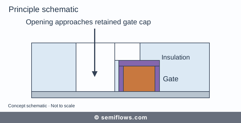
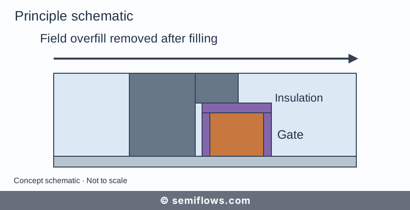
1 (Engineering Practice). Metal Gate Recess: Following the dual-metal gate deposition and chemical mechanical planarization (CMP), the metal gate electrode is selectively recessed down using a controlled isotropic dry or wet etch . This recess step creates a cavity directly above the gate metal . 2. Nitride Etch Stop Deposition: A protective silicon nitride ($SiN_x$) layer is deposited over the entire surface, filling the recessed gate cavity . This step is typically performed using high-conformality atomic layer deposition (ALD) to ensure dense, defect-free gap-fill without voids . 3. Nitride CMP & Planarization: The excess silicon nitride is polished back via CMP, planarizing the nitride stop layer so that it remains localized solely within the gate cavity as a protective cap . 4. Capping Oxide Deposition: An interlayer dielectric oxide layer (the capping oxide) is deposited over the planarized surface . 5. Contact Patterning & Selective Etching: Lithography is performed to define the contact holes (Engineering Practice). Despite overlay offsets where the lithography window overlaps the gate electrode, the subsequent selective contact etch cuts through the capping oxide but stops on the silicon nitride cap and spacer, preventing the exposure of the underlying gate metal [P1, P2]. 6. Contact Metal Fill: A barrier layer and a contact plug metal (historically tungsten, and more recently cobalt or ruthenium) are deposited and subsequently polished back [P2, A1].
+--------------------------------------------------------+
| Lithography Mask (Misaligned) |
| [======] |
+--------------------------------------------------------+
| (Etch oxide selectively)
V
[ Capping Oxide (SiO2) ] [ Capping Oxide (SiO2) ]
======================= =======================
|| [ Nitride Cap (SiNx) ] ||
|| [ Gate Metal ] ||
Spacer ---> || || <-- Spacer
(SiNx) || [ Channel ] ||
-----------++--------------------------++---------------
Source / Drain
Epitaxy (Etch stops here and lands on S/D)
Directional Process Parameter Interactions
In the selective dry etching step, process parameters must be tuned precisely to balance etching kinetics and selectivity . The directional interactions are described as follows:
- Fluorine-to-Carbon (F/C) Ratio: Decreasing the F/C ratio (by using carbon-rich gases like $C_4F_8$ or $C_4F_6$) increases polymer deposition . This directionally improves the selectivity of $SiO_2$ relative to $SiN_x$ . However, if the F/C ratio is too low, "etch stop" or pinch-off occurs within high-aspect-ratio contact holes, preventing the etch from reaching the bottom source/drain contact .
- Polymer-Suppressing Additives: The introduction of oxygen ($O_2$) or hydrogen ($H_2$) modifies the polymer deposition rate . Hydrogen reacts with fluorine to form $HF$, reducing the effective F/C ratio, which enhances polymer protective thickness on $SiN_x$ . Excess hydrogen, however, can over-passivate the $SiO_2$ sidewalls, leading to profile tapering and reduced critical dimensions (Engineering Practice).
- Ion Energy (RF Bias Power): Increasing the RF bias power increases the kinetic energy of the incoming ions . This improves the verticality of the contact profile and helps clear out polymer residues at the bottom of high-aspect-ratio holes . However, higher ion energies increase physical sputtering, which degrades the $SiN_x$ protective cap at the corners, leading to shoulder pulldown and subsequent device shorting .
Challenges & Failure Modes
While the SAC process enables scaling, it introduces severe physical and chemical challenges that can result in yield loss and reliability issues .
1. Contact-to-Gate Shorts due to Corner Loss
During the selective dielectric etch, the top corners of the $SiN_x$ protective cap and gate spacers are exposed to intense physical sputtering . If the etch process selectivity is insufficient or the physical ion bombardment is too energetic, the $SiN_x$ corners are rounded off—a phenomenon known as "shoulder pulldown" . In extreme cases, this corner loss exposes the underlying high-k metal gate stack . When the contact metal is subsequently deposited, a direct electrical bridge forms between the gate and the source/drain contact, causing catastrophic device failure [P1, P2].
2. High-Resistance Failures and native Oxide Residues
For a successful electrical contact, the etch must completely clear the oxide at the bottom of the contact hole to expose the underlying epitaxially grown source/drain silicon [P1, P3]. However, the polymerization required to protect the gate spacers can also lead to polymer accumulation at the bottom of the contact via . If this polymer is not completely removed, or if a native oxide layer reforms on the silicon surface prior to metal deposition, a high-resistance interface is created . This native oxide layer increases the Schottky barrier width and height, causing a severe increase in contact resistance and degrading key circuit parameters, such as the allowed time interval between data-in and the word-line pre-charge ($t_{RDL}$) in DRAM cells [P3, T3]. Advanced cleaning steps, such as plasma native oxide cleaning (PNC), are required to resolve this failure mode .
3. Time-Dependent Dielectric Breakdown (TDDB)
Even if the selective etch does not lead to an immediate physical short-circuit, spacer thinning can severely degrade the long-term reliability of the device . Thinning of the $SiN_x$ spacer reduces the physical distance between the contact metal and the gate electrode . Under high operating electric fields, this localized thin region experiences high electric field stress, accelerating electron trapping and defects generation in the dielectric . This eventually leads to early time-dependent dielectric breakdown (TDDB) between the contact and the gate .
Technology Node Evolution
The implementation of SAC has undergone significant materials and structural evolutions across advanced CMOS technology nodes .
Planar Nodes (e.g., 28nm)
At the 28nm Planar Flow node, contact integration was primarily achieved through conventional lithography and dry etching, where alignment margin was maintained by keeping a relatively wide gate pitch . The self-aligned contact was not yet mandatory for all designs, as the scanner overlay limits were still compatible with the pitch design rules (Engineering Practice).
Early FinFET Nodes (e (Engineering Practice).g., 22nm to 14nm)
With the introduction of the 14nm FinFET node and Intel's pioneering 22nm tri-gate node, the gate pitch scaled below the overlay limits of double-patterning immersion lithography . SAC became an essential integration step . The industry introduced the recessed metal gate capped with a LPCVD or ALD silicon nitride layer [P1, P2]. This scheme successfully isolated the gate from the contact, decoupling transistor performance optimization from overlay margin constraints .
Advanced Sub-7nm Nodes
As scaling progressed to the 7nm FinFET node and beyond, the aspect ratio of the contact holes increased dramatically, resulting in severe aperture pinch-off and contact resistance issues . Traditional tungsten contact metals with titanium nitride ($TiN$) barrier layers reached their scaling limits, as the high-resistivity barrier layer consumed too much of the cross-sectional area of the contact hole [A1, A2].
To address this, advanced nodes have transitioned to cobalt ($Co$) or ruthenium ($Ru$) contact metallization [A1, A2]. Ruthenium, in particular, exhibits low bulk resistivity and acts as its own diffusion barrier, enabling a "barrierless" upper contact structure [A1, A2]. By depositing CVD ruthenium directly onto the dielectric sidewalls and the lower contact, the conductive volume is maximized, which significantly reduces parasitic contact resistance while maintaining excellent reliability under high current densities [A1, A2].
Related Processes
The performance and yield of the SAC modules are deeply interconnected with several adjacent semiconductor manufacturing processes:
- Atomic Layer Deposition (ALD): The deposition of the protective gate spacers and the gate cap dielectric relies on ALD . The exceptional step coverage and precise thickness control of ALD are critical to ensuring uniform protection around the 3D topography of the gate stack, which directly determines the resistance against shoulder pulldown during SAC etching .
- Chemical Mechanical Planarization (CMP): The planarization of both the gate metal recess and the silicon nitride capping layer requires highly selective CMP processes . Non-uniformity in CMP across the wafer can translate into variations in the cap thickness, directly affecting the selective etch margin during contact opening .
- Atomic Layer Etching (ALE): As technology nodes continue to scale, the industry is transitioning from continuous reactive ion etching (RIE) to atomic layer etching (ALE) for the contact opening step . ALE decouples the surface modification and ion activation steps, allowing atomic-scale control over the etch depth and maximizing selectivity between $SiO_2$ and $SiN_x$, which prevents spacer damage .
Future Outlook
Looking toward sub-2nm nodes and the introduction of Gate-All-Around (GAA) nanosheet transistors, self-aligned contact processes are evolving to support even more complex 3D integration schemes . One key trend is the development of Backside Power Delivery Networks (BSPDN), where power contacts are routed from the backside of the wafer, leaving the frontside exclusively for signal routing (Engineering Practice). This requires the fabrication of deep, self-aligned backside contacts that must land precisely on the source and drain epi-layers without disturbing the channel regions . Additionally, research is active on new ultra-low-k spacer materials to replace silicon nitride, aiming to reduce parasitic contact-to-gate capacitance while maintaining the dry etch selectivity necessary to sustain the self-aligned contact paradigm .