Introduction
Modern integrated circuit (IC) architectures rely on complex multi-layer routing networks to connect billions of microscopic transistors on a single chip . Within this multi-level metallization hierarchy, the vertical interconnect access (via) serves as the physical and electrical conduit that bridges conductive pathways across different vertical planes , . Without these vertical pathways, a semiconductor device would remain restricted to two-dimensional planar routing, resulting in severe routing congestion, increased chip area, and degraded signal transmission speeds .
As the industry transitioned through advanced technology nodes—such as the 28nm Planar Flow and the subsequent 14nm FinFET node—the physical dimensions of these vertical connections shrunk dramatically . This scaling has forced engineers to optimize the material systems, physical geometry, and processing sequences of these microscopic channels . Today, managing the aspect ratio, interface cleanliness, and barrier integrity of vertical connections is paramount to maintaining high performance and preventing device failures .
Physics & Mechanism
The fundamental operation of a vertical interconnect access is governed by carrier transport across heterostructural metal-metal and metal-semiconductor interfaces (Engineering Practice). When charge carriers (electrons) traverse a vertical boundary, they encounter interface resistance, commonly referred to as contact resistance ($R_c$) .
Electron Transport and Energy Alignment
At the interface, the mismatch in the work function of the adjacent metals or the metal and semiconductor creates a potential barrier . Carrier injection occurs through two primary quantum-mechanical and thermodynamic mechanisms: 1 (Engineering Practice). Thermionic Emission: Thermally excited carriers overcome the interface energy barrier (Engineering Practice). 2. Field Emission (Quantum Tunneling): Carriers tunnel directly through the thin potential barrier .
To minimize resistance at these interfaces, engineers employ interface engineering, such as modifying the work function using self-assembled monolayers (SAMs) or thin transition metal insertion layers to align energy levels and optimize carrier transmission probability .
High-Aspect-Ratio Mass and Momentum Transport
Creating vertical paths requires high-aspect-ratio etching and metallization , . During the etching phase, reactive ions are accelerated vertically toward the substrate . Momentum transfer from these accelerated ions to the lattice atoms sputters away material, while chemical reactions volatilize the exposed substrate .
During metallization, mass transport mechanisms such as surface diffusion, chemical precursor adsorption, and electromigration-induced atomic transport dictate the quality of the metal fill . In sub-resolution geometries, the transport of metal atoms is heavily constrained by steric hindrance and diffusion limitations within the narrow trenches, often requiring super-filling electroplating techniques or conformal deposition to prevent vacancy accumulation .
Process Principles
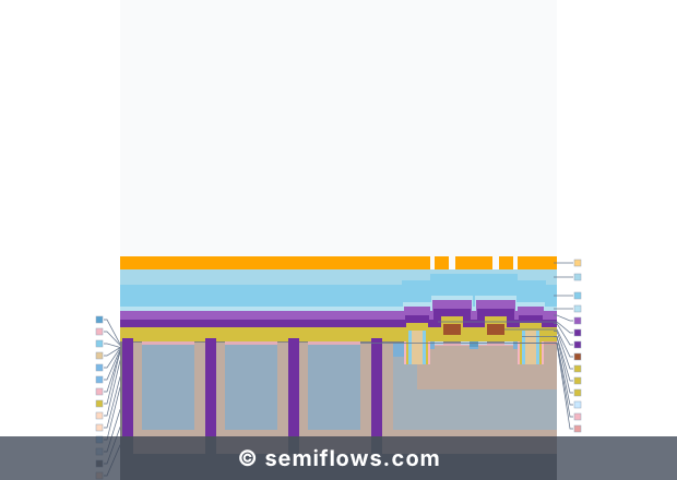
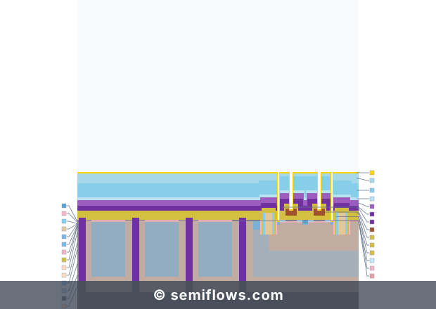
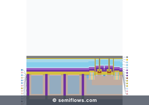
Fabricating a reliable vertical interconnect access involves a sequence of patterning, etching, barrier deposition, and metal filling, where process parameters directionally govern final electrical performance and yield .
Etching Anisotropy and Sidewall Angle
The directional profile of the vertical opening is controlled by the ratio of chemical etching to physical ion bombardment in a process known as dry etching .
- Polymerizing Gas Flow: Increasing the flow of polymerizing passivation gases strengthens protective films on the vertical walls, directionally increasing anisotropy and preventing lateral undercut (Engineering Practice).
- RF Bias Power: Raising the radio frequency (RF) bias power increases the kinetic energy of incoming ions, accelerating the vertical etch rate but also increasing physical damage to surrounding dielectric films (Engineering Practice).
Barrier and Liner Conformality
Prior to bulk metal deposition, a thin barrier layer is deposited to prevent metal diffusion into the surrounding dielectric material .
- Deposition Method: Utilizing atomic layer deposition (ALD) instead of physical vapor deposition (PVD) dramatically improves step coverage and conformality within narrow channels . ALD relies on self-limiting, surface-controlled chemical reactions, which ensure uniform thickness regardless of aspect ratio .
- Aspect Ratio Scaling: As the aspect ratio of the opening increases, precursor diffusion to the bottom of the structure becomes restricted, requiring longer exposure times to prevent local thinning of the barrier .
Electroplating and Super-filling Dynamics
For copper-based vertical interconnects, electrochemical deposition is used to fill the structure (Engineering Practice). The plating bath chemistry contains organic additives (accelerators, suppressors, and levelers) that modulate local current density .
- Suppressor Diffusion: Suppressors diffuse faster to the top opening, inhibiting metal growth there (Engineering Practice).
- Accelerator Accumulation: Accelerators concentrate at the narrowing bottom, promoting rapid bottom-up growth (super-filling) and preventing the formation of central keyhole voids .
Challenges & Failure Modes
As dimensions scale down, the physical reliability of vertical interconnects becomes a dominant factor limiting chip lifetime .
[ Misalignment / Overlay Error ]
|
v
[ Reduced Landing Area & Exposed Dielectric ]
|
v
[ High Local Current Density / Accelerated EM / TDDB ]
Electromigration (EM)
Electromigration occurs when high-density electrical currents cause momentum transfer from conduction electrons to metal ions, physically displacing the atoms in the direction of current flow . This phenomenon is especially severe at the bottom boundary of the vertical interconnect, where current crowds through a narrow contact area . Over time, this atomic transport leads to vacancy condensation, void formation, and ultimate open-circuit failure .
Time-Dependent Dielectric Breakdown (TDDB)
If lithographic alignment fails, the vertical connection may land partially off-target , . This overlay error reduces the effective distance between adjacent metal structures, subjecting the intervening low-k dielectric to higher electric field stress . This accelerated electric field stress degrades the dielectric material, triggering sudden and catastrophic time-dependent dielectric breakdown .
Alignment and Metrology Limitations
Achieving perfect overlay across multiple patterned layers is highly complex . In technologies such as through-silicon via (TSV) integration, conventional processes require an extra zero-mark photolithography step to serve as an alignment guide . To bypass this complexity and reduce costs, advanced integration schemes construct shallow alignment trenches directly in the substrate frame region , . These trenches, shallower than the TSV structures, remain optically recognizable throughout subsequent redistribution layer (RDL) lithography, preventing alignment failures without adding process steps , .
Technology Node Evolution
The materials and integration schemes used to build vertical interconnects have evolved significantly to combat scaling limits .
28nm Planar Node
At the 28nm Planar Flow node, standard copper dual damascene schemes with physical vapor deposited tantalum/tantalum nitride (Ta/TaN) barriers were the industry standard (Engineering Practice). The aspect ratios were low enough that copper electroplating filled the structures with high yield (Engineering Practice).
14nm FinFET Node
With the transition to the 14nm FinFET node, the reduction in lateral spacing drastically increased contact and routing resistance . To sustain electrostatic control, three-dimensional transistor geometries were introduced, complicating the layout and requiring tighter alignment tolerances . Multi-patterning lithography schemes were deployed to define sub-resolution vias, dramatically increasing overlay sensitivity .
7nm Node and Beyond
At the 7nm FinFET node, extreme ultraviolet (EUV) lithography was introduced to simplify multi-patterning schemes and reduce overlay margins . Additionally, traditional copper metallization began reaching its physical limits due to electron scattering at the ultra-thin barrier interfaces . Consequently, advanced nodes have increasingly transitioned to cobalt (Co) or ruthenium (Ru) for local vertical interconnects, as these metals exhibit shorter electron mean free paths and can be filled without thick, high-resistivity diffusion barriers .
Related Processes
The quality of a vertical interconnect is directly coupled to adjacent process steps within the manufacturing flow (Engineering Practice):
- Lithography: Photolithographic precision defines the lateral boundaries and pitch of the vertical path, relying on optical or topographical alignment marks on the wafer to avoid overlay errors , .
- Chemical Mechanical Planarization (CMP): After electroplating or CVD filling, chemical mechanical planarization removes the metal overburden, isolating individual vertical channels and ensuring a flat top surface for subsequent routing layers .
- Dielectric Deposition: Low-k dielectric films must support high-aspect-ratio etching while remaining mechanically stable enough to withstand the thermal and shear stresses experienced during subsequent CMP and metal annealing .
Future Outlook
As traditional dimensional scaling faces thermal and physical limits, the semiconductor industry is moving toward alternative spatial integration architectures , .
Monolithic 3D and 3D Nanofabric
Rather than stacking individual packaging dies, emerging technologies such as 3D Nanofabric processes define multi-layer device structures simultaneously through lateral processing . These architectures utilize shared vertical gates and interconnects built directly within a single monolithic stack, bypassing sequential thermal budgets and improving vertical routing densities .
Backside Power Delivery Networks (BSPDN)
To alleviate routing bottlenecks on the front side of the silicon wafer, advanced nodes are separating power routing from signal routing (Engineering Practice). By shifting the power delivery network to the backside of the wafer, sub-micron "nano-vias" are etched directly through the thinned silicon substrate to contact the source and drain regions from below . This architecture dramatically reduces IR voltage drop, simplifies front-side layout, and represents the next paradigm shift in vertical interconnect technology (Engineering Practice).