Deposition rate describes film-thickness growth per unit time under stated conditions. It is a useful process metric, but rate alone does not determine density, composition, conformality, or gap fill. Those outcomes depend on deposition method, chemistry, surface, geometry, and thermal history. The linked flow labels deposition locations without reporting measured rates.
Where Deposition Rate Acts in the Flow
The free 40nm flow overview includes PMD deposition, SiO hard-mask deposition, and ILD oxide gap fill. Their names indicate integration roles, not rates or the limiting growth regime.
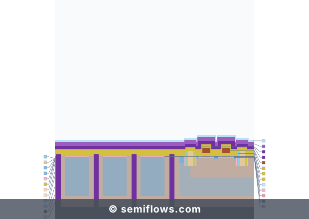

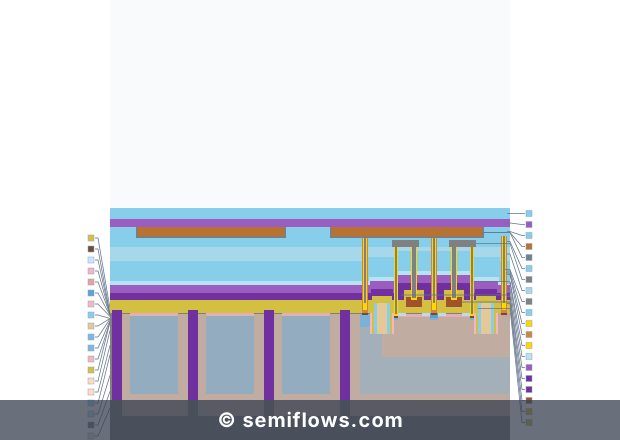
Film-deposition panels do not include measured rates or identify deposition method.
Process checkpoint
Understand SiO Hard Mask deposition in context
Inspect a hard-mask deposition station; the flow does not report its growth rate.
Process context for “Deposition Rate: Meaning and Limits”: 40nm BSI CMOS Image Sensor · F_DTI · Step 12
Physics & Mechanism
Film growth can depend on delivery of reactants or source material, surface reaction, and removal of byproducts . Which process limits the observed rate varies with method and conditions. A measured rate also depends on where and how thickness is sampled. For self-limiting cyclic deposition, growth per cycle and cycle time should be distinguished from continuous film growth per unit time.
Process Principles
A rate comparison needs the same material, method, geometry, measurement location, and thickness definition. Increasing the rate can affect coverage or film properties in a given process, but the direction and size of the effect must be established experimentally. Throughput is also influenced by handling, stabilization, cleaning, and other non-growth time.
Challenges & Failure Modes
Variation across a wafer or between features can obscure a single average rate. A process may meet thickness targets yet fail coverage or composition targets. Conversely, a slower process is not inherently denser or more conformal; these properties require independent measurements.
From Principle to Production Flow
In a real flow, the rate and quality of each selected film must be checked together. The 40nm flow overview provides where deposition occurs but does not publish a rate set point or a limiting mechanism. See CVD, PVD, and ALD for different growth families.
Technology Node Evolution
More complex topography and tighter film requirements increase the value of local coverage and uniformity measurements alongside average rate. A general trend does not imply a universal choice of slower or faster deposition for every later node.
Related Processes
Rate is one descriptor of deposition; thickness, composition, and coverage are separate outputs.
References
Silicon VLSI Technology - Full
James D. Plummer, Michael D. Deal, Peter B. Griffin
Silicon VLSI Technology · ISBN 978-0130850379