Pre-barrier treatment prepares an exposed contact surface before a barrier film is deposited. Depending on the integration, it may remove native oxide or residue and limit interface damage. The available 40nm flow shows nearby contact etch, Ti/TiN liner, and tungsten fill steps, but does not name a distinct pre-barrier treatment. This article explains the interface problem without attributing an unseen cleaning recipe to that flow.
Contact Context for Pre-Barrier Treatment
The free 40nm flow overview shows the surrounding contact module: poly/silicon back etch, Ti/TiN deposition, and tungsten deposition. These labels establish neighboring interfaces, not a documented pre-barrier clean or its chemistry.
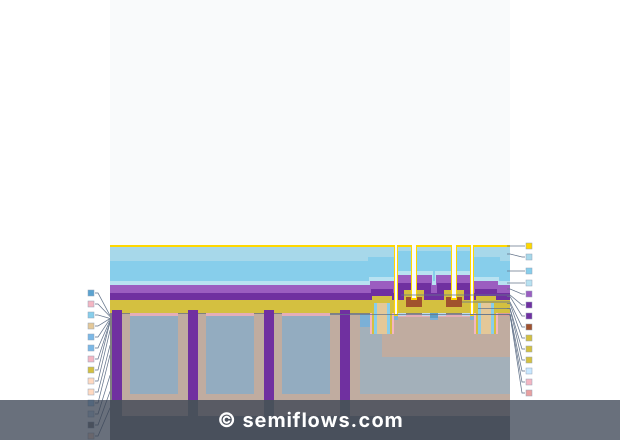
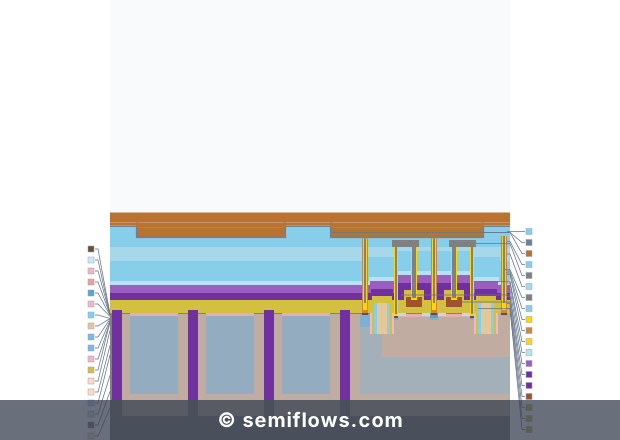
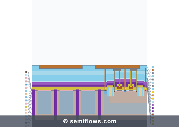
These are neighboring contact steps; the figure does not show a named pre-barrier clean.
Process map
40nm BSI CMOS Image Sensor
Locate contact metallization and barrier roles; the overview does not identify a pre-barrier treatment recipe.
Physics & Mechanism
A contact surface may carry oxide, etch residue, or other contamination when the opening is made. Preparation before liner deposition aims to manage the actual surface without consuming too much of the exposed conductor, dielectric, or junction . The appropriate treatment depends on the material stack; a generic “pre-barrier” label does not prescribe an HF dip, plasma clean, or timed transfer.
A study of a specific an earlier-node logic contact module varied RF pre-clean, Ti/TiN barrier conditions, and tungsten fill, and compared bottom coverage, contact resistance, and junction leakage . It demonstrates that contact electrical outcomes depend on the integrated conditions. It does not show that a separate treatment exists in the linked 40nm flow, or that every oxide regrows immediately on every cleaned surface. Any clean-to-deposit timing claim needs a known surface and ambient.
Process Principles
- Identify the interface: the exposed conductor, residues, and nearby dielectrics define what a preparation step must preserve.
- Separate process stages: pre-clean, liner deposition, and fill can interact but are not the same operation .
- Verify the result: bottom coverage, contact resistance, and junction leakage require distinct measurements.
- Check the route limit: the linked 40nm steps show neighboring operations, not a named pre-barrier treatment.
Challenges & Failure Modes
Residual contamination, unintended surface removal, poor liner coverage, or damage during preparation may affect a contact. The relative risk must be established for the selected stack. The cited contact study reports its own process splits; it does not establish one dominant failure mode for all contacts.
From Principle to Production Flow
A contact integration may place cleaning or surface conditioning between etch and liner deposition, followed by fill and polish. The 40nm flow overview shows the neighboring stations but does not resolve the preparation method. For related mechanisms see surface cleaning, diffusion barriers, and tungsten.
Technology Node Evolution
Changing contact geometry and materials can alter allowable surface loss and coverage. The an earlier-node contact study is a bounded example, not evidence of a universal progression toward one clean or one transfer configuration.
Related Processes
Pre-barrier treatment's neighbors: titanium nitride and diffusion barriers as the barrier it serves; tungsten as the fill that trusts it; surface cleaning and dilute HF as the chemistry it borrows; nickel silicide as the surface-science sibling; and dry etching as the step whose mess it cleans.
Future Outlook
Better interface measurements may help connect preparation conditions with electrical outcomes. Any new treatment should be assessed together with its liner and fill on the intended contact stack.
References
Effect of Contact Plug Deposition Conditions on Junction Leakage and Contact Resistance in Multilevel CMOS Logic Interconnection Device
Yinhua Cui, Jeong Yeul Jeong, Yuan Gao, S. Pyo · Micromachines
Silicon VLSI Technology - Full
James D. Plummer, Michael D. Deal, Peter B. Griffin
Silicon VLSI Technology · ISBN 978-0130850379