Introduction
As semiconductor technology nodes scale down to sub-10nm dimensions, the aspect ratios of isolation trenches, gate structures, and contact holes increase dramatically . Traditional gap-fill techniques, such as high-density plasma chemical vapor deposition (HDP-CVD) and sub-atmospheric chemical vapor deposition (SACVD), reach their physical limits at these geometries (Engineering Practice). These conventional techniques are highly directional or conformal, which leads to premature closure at the top of narrow, high-aspect-ratio trenches, trapping air pockets and forming structural voids (Engineering Practice). To overcome these limitations, the semiconductor industry adopted flowable chemical vapor deposition (FCVD), also known as flowable CVD .
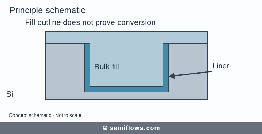
Flowable chemical vapor deposition is a specialized deposition technique where gaseous precursors react in the gas phase or on the wafer surface to form a liquid-like oligomeric film . This liquid-like film flows freely into extremely narrow trenches under the influence of capillary forces and surface tension, enabling a truly bottom-up, void-free gap fill before being cured into a solid dielectric material , . FCVD has become an indispensable process for creating shallow trench isolation (STI) regions in modern fin field effect transistor (FinFET) and gate-all-around (GAA) nanosheet devices , , . It also plays a vital role in 3D heterogeneous integration, local interconnect die isolation, and on-chip passive component manufacturing , .
Physics & Mechanism
The fundamental physical and chemical mechanisms of flowable chemical vapor deposition differ significantly from conventional atomic layer deposition (ALD) or conformal CVD, where film growth occurs via layer-by-layer surface reactions or solid-state condensation . The FCVD process operates via a distinct two-step mechanism: liquid-like deposition followed by chemical conversion .
Oligomerization and Condensation
In the deposition phase, a silicon-containing precursor (typically an organosilane or a silyl-amine compound) is introduced into the chamber along with a co-reactant (such as ammonia, nitrogen, or oxygen radicals generated in a remote plasma system) , . Instead of immediately forming a solid network on the surface, these precursors undergo partial polymerization in the gas phase or at the gas-solid interface, forming low-molecular-weight oligomers (Engineering Practice).
These oligomers—often liquid-like chains containing silicon-nitrogen (Si-N), silicon-hydrogen (Si-H), or silicon-carbon (Si-C) bonds—have a high boiling point and a very low vapor pressure , . Consequently, they condense selectively on the cooler wafer surface (Engineering Practice). Driven by surface tension and capillary action, these liquid-like oligomers flow along the topography, accumulating preferentially at the bottom of trenches and high-aspect-ratio structures to achieve a seamless, bottom-up fill (Engineering Practice).
Conversion and Solidification
Immediately after deposition, the film is not a high-quality oxide but rather a soft, porous, and chemically unstable polymer-like network containing volatile nitrogen- and hydrogen-rich groups , . To convert this temporary liquid-like structure into a rigid, high-density silicon dioxide ($SiO_2$) or silicon nitride ($Si_3N_4$) dielectric, a post-deposition curing and conversion step is required , .
During this conversion phase, the wafer is exposed to an oxidizing environment—such as oxygen ($O_2$), ozone ($O_3$), or steam ($H_2O$)—often facilitated by a rapid thermal annealing (RTA) process or a low-temperature oxygen radical treatment , . The oxygen species diffuse into the porous oligomeric matrix, initiating a chemical substitution reaction . Hydroxyl groups ($-OH$) or oxygen atoms displace the amine ($Si-NH-Si$) or hydride ($Si-H$) linkages, forming a cross-linked silicon-oxygen-silicon ($Si-O-Si$) network , . The volatile byproducts, such as ammonia ($NH_3$) and hydrogen gas ($H_2$), desorb from the film and are pumped away (Engineering Practice). This process results in a dense, solid dielectric layer that conforms to the shape of the trench without preserving any interface boundary , .
Process Principles
The successful execution of flowable chemical vapor deposition depends on the precise balance of process parameters, which directionally affect film flowability, chemical composition, and physical density .
- Wafer Temperature: Unlike traditional CVD, which requires elevated temperatures to drive chemical decomposition, the deposition step in FCVD is performed at relatively low temperatures (Engineering Practice). Lower temperatures promote the physical condensation of oligomers on the wafer surface, enhancing their liquid-like flowability and deposition rate (Engineering Practice). However, if the temperature is too low, the film may contain excessive carbon or nitrogen impurities, leading to high shrinkage rates during conversion (Engineering Practice). Conversely, raising the temperature suppresses condensation, forcing the deposition mechanism toward a conventional conformal CVD mode and increasing the risk of void formation (Engineering Practice).
- Remote Plasma Power: The co-reactants in FCVD are typically activated using a remote plasma source to prevent direct ion bombardment of the delicate wafer structures , . Increasing the remote plasma power increases the concentration of active radicals, which accelerates the initial oligomerization rate (Engineering Practice). This can lead to larger oligomeric molecules that condense faster but have lower flowability due to their increased viscosity (Engineering Practice). Decreasing the plasma power keeps the molecular weight of the oligomers lower, prolonging their flowable lifetime and improving gap-fill performance in extremely narrow trenches (Engineering Practice).
- Precursor Flow Ratio: The ratio of the silicon-containing precursor to the co-reactant gas directly impacts the chemical composition of the condensed film (Engineering Practice). Increasing the silicon precursor flow relative to the co-reactant increases the deposition rate but often leads to an incomplete gas-phase reaction, yielding a film with high organic content or hydrogen density (Engineering Practice). This subsequently increases the volumetric shrinkage and mechanical stress of the film during the final curing phase (Engineering Practice).
- Chamber Pressure: Higher operating pressures in the deposition chamber increase the collision frequency of gas-phase molecules, promoting oligomerization and increasing the deposition rate (Engineering Practice). However, if the pressure is set too high, gas-phase nucleation can occur, leading to particle contamination and non-uniform film morphology (Engineering Practice).
Challenges & Failure Modes
While flowable chemical vapor deposition solves the fundamental gap-fill limit of traditional CVD, it introduces unique mechanical and chemical challenges during the conversion of the fluid phase to a solid phase .
Volumetric Shrinkage and Stress
The most critical challenge in FCVD is volumetric shrinkage . During the steam or oxygen curing phase, the dense, low-molecular-weight network expels volatile species such as $NH_3$ and $H_2$ as it transitions to silicon dioxide . This chemical reconstruction results in a substantial reduction in volume, creating high tensile stress within the trench (Engineering Practice).
If the tensile stress is not carefully managed, it can cause several failure modes: 1 (Engineering Practice). Cracking and Delamination: The internal tensile stress exceeds the mechanical strength of the film, leading to micro-cracks or separation of the FCVD oxide from the trench walls (Engineering Practice). 2. Fin Bending: In high-aspect-ratio FinFET structures, the shrinking dielectric pulls on the adjacent silicon fins, causing them to bend or collapse, which alters the electrical characteristics of the device (Engineering Practice). 3. Stress-Induced Voids: If the outer surface of the FCVD film solidifies and densifies before the bulk of the film in the trench can undergo conversion, volatile byproducts become trapped . This results in localized pressure build-up and stress-induced voiding inside the trench (Engineering Practice).
Wet Etch Rate Ratio (WERR) Degradation
For a deposited oxide to function effectively in integrated circuits, it must match the physical and chemical quality of thermal oxide (Engineering Practice). This quality is typically evaluated using the wet etch rate ratio (WERR), which compares the etch rate of the deposited film in dilute hydrofluoric acid (DHF) to that of high-quality thermal silicon dioxide , .
Due to the diffusion limit of oxidizing species, the bottom of deep, narrow trenches often suffers from incomplete chemical conversion during curing , . These region-specific defects leave behind residual Si-N, Si-H, or Si-OH bonds , . Consequently, the bottom of the trench exhibits a significantly higher wet etch rate than the top (Engineering Practice). During subsequent etching or cleaning steps, the acid penetrates the partially converted lower regions, causing rapid, uncontrolled lateral etching—commonly referred to as trench recessing or "keyhole" exposure , , .
Technology Node Evolution
The role and implementation of flowable chemical vapor deposition have evolved continuously across major technological milestones to support advanced device scaling .
28nm Planar 14nm / 7nm FinFET 3nm GAA Nanosheet
(Planar STI Fill) ───> (High Aspect Ratio Fins) ───> (Inner Spacer & Gate-Cut)
- Simple Gap Fill - Severe Aspect Ratios - Dielectric Plugs
- Low Shrinkage - Fin Bending Mitigation - Air-Gap Integration
28nm Planar Node
At the 28nm planar node, the aspect ratios of shallow trench isolation structures were moderately challenging . FCVD was introduced to replace high-density plasma deposition in the most demanding isolation trenches to prevent voiding . At this node, simple low-temperature thermal curing was sufficient to achieve acceptable film quality and low shrinkage, as the trenches were relatively wide and shallow (Engineering Practice).
14nm to 7nm FinFET Nodes
With the transition to 14nm FinFET and 7nm FinFET architectures, the aspect ratios of the isolation trenches separating adjacent silicon fins escalated beyond 10:1 , . Under these conditions, the mechanical stress generated during FCVD oxide shrinkage became a severe threat to structural integrity . Process engineers optimized the conversion step by implementing multi-step curing recipes—using cyclic low-temperature oxygen radical treatments followed by high-temperature steam annealing—to slowly densify the film and minimize fin bending , .
GAA Nanosheet and Beyond
In gate-all-around nanosheet architectures, the integration density and structural complexity reach extreme levels , . Here, FCVD is utilized not only for conventional STI fill but also for isolating complex gate segments through "gate-cut" processes . In these processes, continuous metal gates are divided into isolated sections by etching deep recesses and backfilling them with high-quality FCVD oxide dielectric plugs to maintain structural and electrical isolation .
Furthermore, FCVD plays a crucial role in creating advanced air-gap inner spacer designs . By combining selective dry etching with controlled deposition and recessing of FCVD sacrificial layers, manufacturers can form and seal air gaps between the gate and the source/drain regions , . These air gaps leverage the ultra-low dielectric constant of air to dramatically reduce parasitic capacitance and boost high-frequency transistor switching speeds .
Related Processes
Flowable chemical vapor deposition does not operate in isolation; it is highly integrated with several key upstream and downstream process modules in the semiconductor manufacturing flow .
- Dry Etching: After FCVD oxide deposition and curing, the excess overburden must be recessed to expose active areas , . Advanced reactive ion etching (RIE) techniques are used to selectively recess the oxide with high precision, ensuring the active silicon fins or nanosheets are not damaged during the exposure step , , .
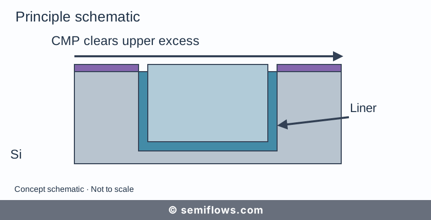
- Chemical Mechanical Planarization (CMP): Because the liquid-like deposition of FCVD leaves a highly planarized surface, it reduces the overall topography variation across the wafer , . Subsequent chemical mechanical planarization steps can easily polish back the remaining oxide overburden to achieve global planarity, exposing the underlying active structures with minimal dishing or erosion defects , .
- Rapid Thermal Annealing: Thermal processing is the bridge that converts the unstable liquid-like oligomer into a highly dense, robust dielectric network . High-temperature steam or oxygen annealing drives out the nitrogen and hydrogen byproducts, cross-linking the silicon-oxygen bonds and reducing the wet etch rate to match that of high-quality thermal oxide , .
Future Outlook
As the semiconductor industry advances toward high-NA (numerical aperture) lithography, backside power delivery networks (BSPDNs), and 3D monolithic stacking, the demands on flowable chemical vapor deposition continue to expand . Future developments are focused on exploring novel organosilicon precursors that exhibit lower volumetric shrinkage and generate fewer volatile leaving groups, thereby mitigating tensile stress during conversion (Engineering Practice).
Additionally, research is ongoing to expand flowable CVD chemistry beyond silicon oxides and nitrides . Developing flowable low-k dielectrics, flowable metals, and flowable high-k materials will open up new pathways for bottom-up metallization and advanced dielectric isolation in complex, multi-layered 3D structures, ensuring that FCVD remains a cornerstone of sub-2nm semiconductor integration .