How a chip is built
Semiconductor manufacturing builds devices and their connections on a wafer through repeated cycles of adding material, defining patterns, removing selected regions and changing material properties. Lithography specifies where a change should happen; deposition and etching help create the structure. A complete chip also needs electrical connections, testing and packaging. One pass through these operations does not make a finished circuit.
The useful starting point is the structure being made. First locate the transistor, then the contact joining it to wiring, then the metal network connecting many devices. This map explains their relationship without treating one company's process sequence as universal.
Process map
28nm Planar Flow
Locate isolation, gate, contact and metal modules in the 28nm planar overview; use their order as a reference integration sequence.
Read the manufacturing map
The diagram separates device formation, local connections and wiring. The repeating operations below it can appear in more than one region of the flow. For example, a deposited dielectric can isolate neighboring devices or insulate neighboring metal lines; the material family alone does not identify its job.
| Part of the flow | What is being built | Question to ask |
|---|---|---|
| Device formation, often called FEOL | Isolation, wells, gates and source/drain regions | What controls current, and what keeps devices separate? |
| Device contacts and local connections, often grouped as MOL | Electrical access to the transistor terminals | Which device region is being connected? |
| Interconnect, usually called BEOL | Metal lines, vias and insulating layers | Which circuit nodes must connect without shorting? |
| Test and packaging | A tested die and its external connections | Can the die function and connect to the surrounding system? |
FEOL, MOL and BEOL are useful organizing labels, not a guarantee that every process owner draws the boundaries in the same place. This article uses MOL for the device-to-wiring transition. Packaging can also be called a back-end activity; that usage should not be confused with wafer-level BEOL wiring.
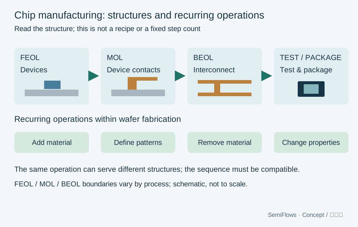
Conceptual teaching diagram; independently drawn from the cited principles, not a course process section.
Why patterning repeats
A transistor and the wires above it require different shapes in different materials. A typical patterning cycle coats a surface with photoresist, exposes and develops a pattern, transfers that pattern into an underlying material or uses it as a mask, and removes resist when its job is finished. A later layer needs its own pattern and alignment to existing features.
This is why “lithography makes the chip” is incomplete. Exposure creates a spatial instruction in a resist system. The following material-changing operation determines what remains in the wafer. Etch selectivity, surface condition and alignment all matter to the result; an image in resist is not yet the final electrical structure.
Read photolithography principles, photoresist and resist removal as three connected parts of this cycle.
Why deposition is not one interchangeable step
Deposition adds a film, but the required film depends on the task. Covering the walls of a narrow feature, filling its interior and creating a conductive layer are different requirements. A coating can follow a surface well yet close a gap before its interior is filled. Conversely, a process intended for filling may require later treatment before the material has its final properties.
CVD, PVD and ALD describe different ways of supplying and incorporating material. Their names alone do not prove that a particular film meets a device's electrical or geometric requirements. Compare the mechanism with the location of the film in the flow.
Why the order matters
Each operation inherits what earlier operations left behind. Heating, cleaning, implantation or etching can affect structures that already exist. A step that makes a good isolated film can still be unsuitable after a sensitive material has been introduced. Process integration is the work of making the sequence compatible, including subsequent operations.
Contacts illustrate the connection between physical structure and circuit purpose. A gate may control a channel correctly, but the circuit still needs low-resistance access to the device terminals and a wiring network that does not short adjacent nodes. Device formation and interconnect therefore solve connected, distinct problems.
Use a real flow as a reading exercise
Open the 28nm planar flow overview and locate isolation, gate formation, contacts and metal layers. For each region, name the structure produced and one earlier structure that must survive. The overview provides a reference fabrication sequence; this article supplies the high-level map. Other device architectures and image sensors require additional or different modules.
You have understood the map when you can explain why deposition and lithography recur, distinguish a contact from a metal line, and follow one electrical connection from a device toward upper wiring. Memorizing a fixed number of “chip-making steps” is less useful than recognizing those dependencies.
References
Silicon VLSI Technology - Full
James D. Plummer, Michael D. Deal, Peter B. Griffin
Silicon VLSI Technology · ISBN 978-0130850379