Three names describe when TSV formation enters the flow
Via-first, via-middle and via-last classify through-silicon via (TSV) integration by its position relative to transistor fabrication and on-chip interconnect fabrication. In the convention used by Burkett and colleagues, via-first precedes front-end-of-line (FEOL) device processing, via-middle follows FEOL and precedes back-end-of-line (BEOL) interconnect processing, and via-last follows both. The names describe a sequence choice, not three different electrical functions.
A TSV provides a conducting route through silicon. Its integration schedule must account for structures already present and processes still to come. This article compares those dependencies; it does not select a manufacturing route or provide processing settings.
Process map
40nm BSI CMOS Image Sensor
Locate device-formation and metal-interconnect modules in the free CIS overview; use it as a module-boundary exercise, not evidence of a TSV route.
Read the insertion points
The diagram shows three alternative schedules. Each row is a separate option, not a sequence of three TSV operations on one wafer. “TSV formation” marks the integration module; it does not claim that every finishing or backside exposure operation is completed at that instant.
| Integration label | What precedes the TSV module? | What follows it? | Main compatibility question |
|---|---|---|---|
| Via-first | The relevant FEOL device sequence has not yet occurred | Device formation and BEOL wiring | Can the chosen TSV materials and structure tolerate the later device processes? |
| Via-middle | FEOL devices | BEOL wiring | Can TSV formation preserve the existing devices, and remain compatible with subsequent wiring? |
| Via-last | FEOL devices and BEOL wiring | Remaining integration and assembly operations | Can TSV formation preserve both the devices and the completed wiring stack? |
The table is a reading aid for the cited convention. A diagram with only a finished cross-section does not establish which schedule was used. Locate the TSV module in the actual process history before assigning a label.
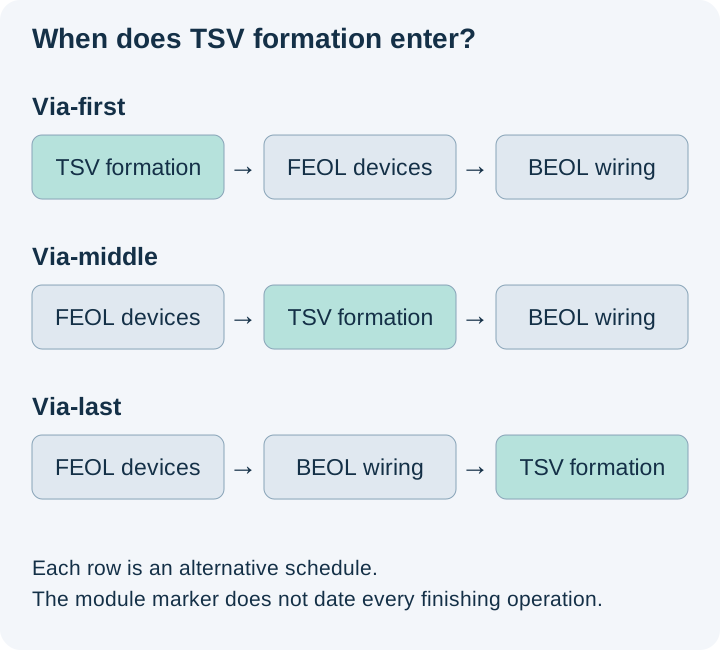
Original concept schematic; not a course cross-section or manufacturing recipe.
Why timing changes the constraints
Via-first leaves more freedom during initial TSV processing because the transistors have not yet been fabricated. That freedom is conditional: the TSV materials must then survive the later device-processing environment. A material that is convenient to deposit at the beginning is not automatically compatible with everything that follows.
For via-middle and via-last, previously fabricated structures impose constraints on the new operation. In the tutorial's examples, liner deposition and other TSV operations must be compatible with the thermal limits of the structures present at that point. The distinction is not simply “earlier is hotter” or “later is better.” Compatibility depends on the actual stack and complete sequence.
Separate timing from the hole and film roles
The tutorial illustrates TSV formation starting with a blind opening in silicon. The opening need not pass through the entire starting wafer when first etched; subsequent processing can expose the other end. Thus “through-silicon” describes the resulting connection, not proof that the first etch went through the full wafer.
In the copper-filled examples, the insulating liner separates the conductor electrically from silicon, a barrier limits unwanted material transport, and a seed layer supports subsequent metal deposition. These are different functions. The via profile and film coverage affect whether those functions can be maintained along the opening. A visible hole alone is not a completed electrical connection, and a timing label does not specify the liner, fill material or geometry.
Do not confuse two uses of via-first
In via-first versus trench-first dual damascene, “first” compares the preparation of a via and a trench within an interconnect dielectric. Here, “first” places TSV formation relative to the FEOL and BEOL stages. These are different comparisons; a dual-damascene via-first label does not identify the TSV integration schedule.
A sequence-reading exercise
Three hypothetical process records describe the moment TSV formation begins:
- A: transistors are present, but the multilayer BEOL wiring has not been fabricated.
- B: both transistors and BEOL wiring are present.
- C: the FEOL transistor sequence has not yet begun.
Using the convention above, A is via-middle, B is via-last and C is via-first. Now change the question: which route has the best yield? None of the records answers it. A schedule establishes dependencies, while yield requires evidence about the implemented structure and its defects. The exercise is constructed from the definitions, not production data.
For a separate exercise in reading module boundaries, open the 40nm CIS overview and locate device formation and metal interconnect modules. That overview provides a fabrication map; it is not a documented comparison of the three TSV routes. The manufacturing process map provides broader context.
Original source
- Burkett and colleagues, Tutorial on forming through-silicon vias, 2020. Its integration definitions and illustrative film roles support this comparison; its specific process settings are not prescriptions for the linked course.
References
Tutorial on forming through-silicon vias
S. Burkett, M. Jordan, R. Schmitt, L. Menk, A. Hollowell