How a CMOS image sensor turns light into a signal
A CMOS image sensor converts absorbed light into charge, stores that charge during exposure and reads an electrical signal from each pixel. In a common four-transistor pinned-photodiode pixel, charge collects in the photodiode, moves through a transfer gate to a floating diffusion, and changes that node's voltage. Readout circuitry senses the voltage; it does not carry the original photoelectrons through the source-follower gate.
This article follows that signal path. It separates light collection, charge transfer and voltage readout, then explains how frontside and backside illumination relate to the same basic pixel task.
Process map
40nm BSI CMOS Image Sensor
Locate frontside fabrication, interconnect, bonding, thinning and backside preparation in the 40nm BSI overview; distinguish fabrication order from pixel timing.
Follow charge first, then voltage
The conceptual diagram shows a pinned photodiode (PPD), transfer gate (TG), floating diffusion (FD), reset transistor (RST), source follower (SF) and row select (SEL). It represents a common four-transistor pixel, not every CMOS sensor design. Shared-pixel arrangements can reuse readout devices.
During exposure, absorbed photons can generate electron–hole pairs in silicon. The pixel's fields and potential profile help collect signal electrons in the photodiode. The stored signal depends on collected charge, not simply the number of photons arriving at the sensor surface: some light is reflected or absorbed elsewhere, and not every generated carrier contributes to the signal.
When TG opens the transfer path, the stored charge moves to FD. The source follower senses FD's voltage through its insulated gate, and row selection connects the readout path to a column. The solid charge-transfer arrow and dashed voltage-sensing connection in the figure are deliberately different.
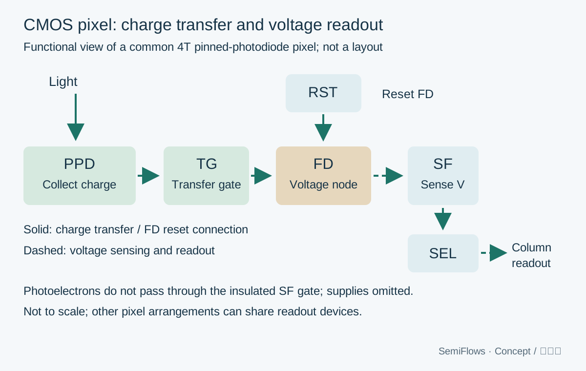
Conceptual teaching diagram; independently drawn from the cited principles, not a course process section.
Read the pixel in sequence
| Operation | Physical change | What the readout uses |
|---|---|---|
| Integrate light | Signal charge accumulates in the PPD | The stored charge is not yet the final output voltage |
| Reset and sample FD | RST establishes the FD reset level | A reference sample |
| Transfer charge | TG allows charge to move from PPD to FD | FD voltage changes |
| Sample the signal level | SF and SEL provide access to that voltage | Signal and reset samples can be compared |
In a simple small-signal description, the magnitude of FD voltage change is approximately collected charge divided by effective FD capacitance. The sign depends on the charge and voltage convention. Larger capacitance gives a smaller voltage change for the same transferred charge; conversion gain is therefore distinct from the photodiode's ability to collect light.
Correlated double sampling compares appropriate reset and signal samples to suppress certain correlated noise components. It does not eliminate photon shot noise or every source of sensor noise. Readout architecture and timing determine what is actually cancelled.
What the pinned photodiode contributes
The PPD stores charge in a buried region with a pinned surface. Its electrostatic structure helps manage surface-related dark current and enables efficient transfer when the pixel is designed and operated appropriately. It is not merely a light-sensitive capacitor with arbitrary wiring.
Charge must also leave the storage region. A potential barrier, a poorly shaped transfer path or trapping can leave residual charge and cause image lag. Consequently, good light collection alone does not prove good image quality. The transfer structure and readout must preserve the signal as well.
Frontside and backside illumination
In frontside illumination, light enters from the side carrying the transistor and interconnect structures. In backside illumination (BSI), light enters from the opposite side after the wafer structure has been prepared for that path. This changes how the optical path encounters frontside wiring; it does not remove the need for a photodiode, charge transfer and electrical readout.
BSI performance still depends on absorption, carrier collection, backside surface treatment and pixel isolation. It should not be reduced to “moving wires guarantees a better sensor.” The 40nm BSI process overview connects these concepts to fabrication. Wafer thinning and bonding before thinning explain two integration tasks, while STI versus DTI distinguishes isolation structures.
Check your understanding on a sensor flow
Use the 40nm BSI course overview to locate frontside device fabrication, interconnect, bonding, backside thinning and backside preparation. That is a manufacturing sequence, not the pixel's exposure-and-readout timing sequence. Keeping these two sequences separate prevents a common confusion: wafer thinning happens during fabrication, whereas charge integration and transfer repeat while the sensor operates.
Return to the diagram and trace two paths: the photocharge path from PPD to FD, and the voltage-sensing path from FD through readout. If an explanation sends the photoelectrons through the SF gate, it has mixed those paths. If it attributes every noise improvement to BSI, it has mixed the optical architecture with readout behavior.
References
A Review of the Pinned Photodiode for CCD and CMOS Image Sensors
E. Fossum, Donald B. Hondongwa · IEEE Journal of the Electron Devices Society