Follow the boundary a connection crosses
An interconnect can join features inside one die, connect separate dies, or connect a package to a board. These are different physical boundaries. “Via,” “redistribution layer,” “interposer,” and “bond” describe different parts of that path; they are not interchangeable names for an increasingly advanced metal layer.
Start with two questions: what does this connection join, and what material or interface does it cross? An on-chip interlayer via crosses a dielectric between wiring levels. A through-silicon via passes through silicon. A bonded interface joins previously separate surfaces. A routing structure such as an RDL or interposer can carry lateral connections. Those functions may coexist in one assembly.
Process map
40nm BSI CMOS Image Sensor
Locate the CIS metal-interconnect, wafer-bonding and backside-processing modules; keep that fabrication map distinct from a complete package assembly flow.
A map of the connection levels
The diagram is an original functional sketch, not a product cross-section or a manufacturing sequence. Its boxes distinguish functional boundaries: an assembly does not necessarily contain every element.
| Level or structure | Useful question | What the name alone does not establish |
|---|---|---|
| On-chip metal and vias | Which circuit features or metal levels are joined? | How another die is attached |
| Die pads and bonded joints | Where does the signal leave a die or cross a bond? | The entire package routing topology |
| RDL or interposer routing | How are connection locations redistributed or dies linked? | That a full silicon interposer is always required |
| TSV | Which silicon body is traversed vertically? | A lateral routing layer or a complete bonding method |
| Package-to-board connection | How does the assembly connect outward? | The internal die-to-die interface |
A vertical line in a drawing is not enough to identify a TSV: check whether it crosses silicon or only an insulating film. Similarly, the presence of copper does not identify the connection level.
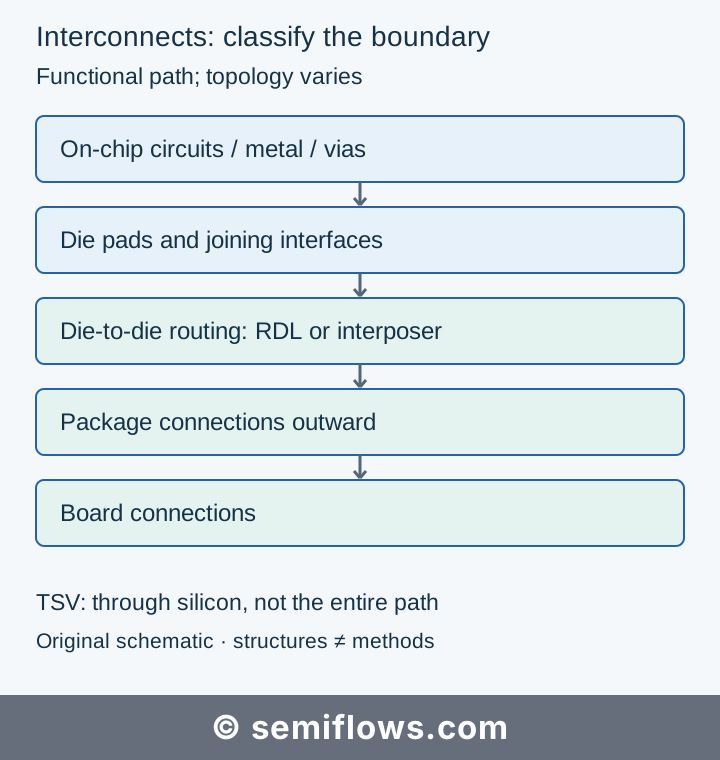
Original concept schematic; not a course cross-section or manufacturing recipe.
Why package routing cannot be read from the node name
A transistor technology name describes a different design dimension from a package's die-to-die routing. The cited packaging presentation contains examples using a bridge die and examples using redistribution routing without a bridge. It demonstrates that more than one physical arrangement can connect chiplets. Its vendor-specific comparisons are not a universal ranking or a process recommendation.
On-chip wiring also has its own electrical isolation and integration requirements. The textbook separates conducting levels from the dielectrics between them. Moving a signal beyond the die introduces additional structures and interfaces; calling everything “BEOL” obscures which boundary must actually be inspected.
Three counterexamples to common shortcuts
“All vias are TSVs.” A via through an intermetal dielectric need not pass through silicon. Classify it by the body it crosses.
“Chiplets require a full silicon interposer.” The reviewed source includes bridge-based and RDL-only examples. Establish the actual topology before drawing the connection path.
“A bond is the package.” A bond joins a particular interface. It does not by itself explain lateral routing, external connections, or every other interface in the assembly. A complete path can contain several of these structures.
Trace one signal yourself
Sketch two dies. Mark a source circuit on die A and a destination circuit on die B. Draw each conductor and interface separately. Label an on-chip path, the exit pad, the joining interface, and the route between the dies. Add a TSV only if your hypothetical route actually traverses silicon. State any topology you assumed.
Then erase one element and ask whether another valid topology can perform the same connection. This exercise reveals why a list of packaging terms is insufficient: the terms must form a physically continuous path.
For a bounded fabrication example, use the 40nm CIS overview. Locate its metal-interconnect modules and subsequent wafer-bonding and backside-processing stages. The public overview provides that module map; it is not a complete chiplet-packaging or HBM course. The manufacturing process map provides the broader fabrication context.
Sources
Plummer, Deal and Griffin, Silicon VLSI Technology, chapter 11, especially the distinction between conductors and intermetal dielectrics. ISBN 978-0130850379.
Davis and Olson, Scaling Interconnect Densities Meeting the Growing Demand for Chiplet Integration, IMAPS, 2023. Original publication. Used for concrete alternative connection topologies, not its commercial comparisons or projected specifications.
Burkett et al., Tutorial on forming through-silicon vias, Journal of Vacuum Science & Technology A 38, 031202, 2020. Original publication, abstract and introduction. Used for through-substrate connections and vertical chip-to-chip routing, not fabrication parameters.
References
Silicon VLSI Technology - Full
James D. Plummer, Michael D. Deal, Peter B. Griffin
Silicon VLSI Technology · ISBN 978-0130850379
Scaling Interconnect Densities Meeting the Growing Demand for Chiplet Integration
Robin Davis, Tim Olson · IMAPSource Proceedings
Tutorial on forming through-silicon vias
S. Burkett, M. Jordan, R. Schmitt, L. Menk, A. Hollowell